6.7 Billion pixels per second image readout? Check. 240fps hardware-based object-recognition and tracking? Check.
Without question, the Samsung NX1 was truly one of the standout products at the Photokina 2014 tradeshow in Cologne, Germany, with top-notch performance, a sophisticated hybrid autofocus system, and an amazing “auto-shot” mode that can capture a baseball in flight at the exact moment it’s coming off the bat.
With its amazing speed and rugged build quality, the Samsung NX1 is clearly aimed at attracting professionals to the NX-mount, and it just might do that, if it tests as well in the lab and in the field as it shows in the tradeshow booth.
Jay Kelbley, Senior Marketing Manager, Digital Imaging, Samsung Electronics
During the show, Imaging Resource publisher and founder Dave Etchells met with Samsung Electronics senior marketing manager for digital imaging, Jay Kelbley, for a wide-ranging discussion of the Samsung NX1, its cutting-edge technology, and why the company feels its offering to be unique in the marketplace.
What followed was a fairly technical discussion of just what Samsung has managed to pack inside the NX1’s diminutive body, and some of its capabilities are pretty eye-popping. Read on for the details:
Dave Etchells/Imaging Resource: As you’d expect, I have a lot of questions about the Samsung NX1 and the technology in it, starting with autofocus. You make some really impressive claims for autofocus speed and capability, but on-chip phase detect isn’t free of trade-offs. I wanted to talk about some of those and how Samsung’s addressed them, or to what extent.
Jay Kelbley/Samsung Electronics: Sure.
DE: One obvious thing is that PDAF involves shading some of the pixels so they see light coming from just one side of the lens or the other. It’s not a big problem, you can always bump up the gain in that pixel to compensate for the half of the light it’s not seeing, but you guys have got of pixels and they’re also cross-points.
JK: Sure.
DE: At what point or when does it become an issue with image quality, having so many focus pixels? Another way of asking that is what percentage of the pixels really are focus pixels?
JK: Well, even when you’ve got more than 200 phase-detect points, compared to 28 megapixels total, the percentage of AF pixels is miniscule.
DE: Ah, OK. [Here’s a little back-of-the-envelope, are-we-in-the-right-ballpark math to illustrate this: Let’s assume that each focus point uses 500 pixels in each direction, or 1,000 pixels total. That’d mean 200,000 pixels across the sensor, out of a total of 28 million, or just 0.7%, and my assumption of 500 pixels in each direction is almost certainly overly generous.]
Phase-detect AF uses differences in the position of light rays coming from opposite sides of the lens to determine out of focus conditions. It thus knows not only that the subject is out of focus, but by how much. Here’s a page that explains phase-detect AF in more detail.
Dave Etchells/Imaging Resource: 如你所料,我有一堆关于三星NX1和它所使用的技术的问题,让我们从自动对焦开始。你们宣称了令人印象深刻的自动对焦速度和能力,但是芯片相位检测是需要权衡的,我想谈一些这个方面的以及三星是怎么解决的,或者做到了什么程度。
Jay Kelbley/Samsung Electronics: 好的。
DE: 一个显见的事实是,相位对焦需要遮挡一部分像素才能接收镜头一边或另一边的光线,这不是很大的问题,你可以随时提高那个像素的信号,补偿另一半看不到光线,但是你们有数量巨大的对焦点并且他们都是十字型的。
JK: 没错。
DE: 在有那么多的对焦像素的情况下,什么时候会影响到画质呢?换个问法就是,百分之几的像素其实是对焦像素?
JK: 唔,即使你有超过200个相位对焦点,和2800万像素比起来,对焦像素的比例是微乎其微的。
DE: 哦,好的。 [这里用一个简便计算、估算来解释:我们假设每个对焦点在每个方向上使用500个像素,或者说一共1,000个像素,这就意味着传感器上有20万像素,在2800万像素里只占0.7%,而且我每个方向500个像素的假设肯定是太多了。]
JK: As we’re going up in resolution, we have some advantages relative to current sensor technology in fill. Our fill efficiency is much higher than most of the industry, thanks in large part to moving to 65nm design rules for our latest sensor. [A nanometer (nm) is one billionth of a meter (10-9 meters), or one millionth of a millimeter. While things like memory circuits have even smaller design rules, 65nm is unusually small for a sensor chip.]
DE: But it’s backside-illuminated, so it’s collecting all the light anyway. [The point of this comment is that Jay was talking about smaller design rules (minimum feature size on the sensor chip) as contributing to a higher fill ratio, or percentage of the silicon area that’s able to collect light. This was confusing, because as I had understood it, the whole point of BSI is that all the peripheral circuitry doesn’t matter, so you could theoretically get a 100% fill factor. If that’s the case, why would smaller design rules be a benefit here? Read on for the answer.]
DE: 但是它是背照式的,不管如何它都会收集所有的光线。 [这么说的关键是Jay在谈论更小的设计线宽(传感器芯片上的最小特征尺寸)是为了实现更高的填充率,或者说参与感光的芯片面积所占的比例。这让我混乱了,因为我所理解的是:整个BSI的重点是所有的外围电路已经无关紧要(因为都放到光电二极管下面去了,译者注),理论上你能获得100%的填充率。如果是这样的话,为什么更小的设计线宽会带来好处呢?答案请继续阅读。]
JK: It’s collecting all…
JK: 它收集所有的……(肯定DE的说法,译者注)
DE: So with the smaller design rules, you’ve got a bigger capacitor, essentially, to store it on? Is that what it is? Or a bigger potential well? [Again, I was trying to understand what the consequence of smaller design rules meant. I was wondering if it meant they were able to create a potential well that could hold more electrons, which would contribute to lower noise levels.]
DE: 所以靠着更小的设计线宽,基本上能获得更大的电容来接收光线?是这样吗?还是有更大的潜力? [再一次,我试着弄明白更小设计线宽的意义。我在想是不是意味着能做出一个储存更多电子的电位阱,这样有助于降低噪点水平。]
JK: Well, we can make much more efficient structures, smaller structures, so the net result is we can get better fill in general. We don’t have to make big, thick walls on everything. As well, when we switch to copper [replacing polysilicon for the wiring on the chip], we’ve moved to a much more conductive material, which helps us in heat dissipation, it helps us in…
DE: Propagation of the signals across the chip? [Meaning potentially faster readout speeds]
DE: 芯片更快地传递信号?[意思是可能有更快的读取速度]
JK: …reducing resistance. So we’re using less material, so again, even though we’re BSI, we’re cutting the pixel depth even more that way, which gives us more sensitivity and efficiency. So you’ll find when you actually get these to test that the high ISO noise on these is much lower than it should be, if you follow the curve down in terms of pixel pitch, because of BSI, because of copper, because of the more efficient microlenses we’ve put on. The microlenses on these appear to cover almost 100%.
If you looked at the NX30 microlens, you’d say it looks to have 95%-ish coverage. For a square microlens it’s pretty good; these things look visibly to be very close to 100% when you look at them on a microscope cutaway. So we’re still making lots of incremental improvements and we’re making them in technology vectors that no one else is. As far as I know, no other camera manufacturer is running a copper process for their sensors, and I don’t believe any are running design rules close to these. I believe that some manufacturers, making higher-end cameras, are still running their processes in the range of 300nm design rules.
Copper metallization has been around the IC industry for years now – the photo at left is courtesy IBM Corporation, circa 1997.
Because copper is 40% more conductive than aluminum, it can increase circuit speeds and reduce power consumption. As far as we know, Samsung is the first sensor maker to use copper metallization.
This contributes to the NX1’s amazing speed, and the ability to track fast-moving ojbects without melting the sensor in the process 🙂
DE: By semiconductor standards, that’s enormous.
DE: 按半导体的标准,这差异是巨大的。
JK: That’s really large, and for memory structures, for computing structures, you can be down in the teens. So it’s my understanding that we have the tightest design rules of any sensor manufacturing process used for cameras by a factor of two, and by general average probably close to a factor of four or five.
DE: It’s interesting what you had mentioned, you know, you were talking about the “big thick walls”. I just realized you were talking about the isolation diffusions between the pixels not taking up as much space with the smaller design rules, so even when you look at the backside-illuminated structure — I’d been thinking that you’ve got 100% of the surface area available, but you still have to separate the photodiodes from each other, and that’s where the smaller design rules come in.
DE: 你之前谈到的关于“又大又厚的墙”很有趣,我才发现你是在说像素之间的分隔区因为更小的设计线宽而不会占用太多的空间,当你观察背照式结构——我一直以为你们获得了100%有效表面积,但其实你们还是要分隔开每个光电二极管,这就是更小的设计线宽发挥作用的地方了。
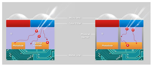
Samsung’s ISOCELL process, developed for cell phone sensors reduced “crosstalk” between pixels by inserting a reflective barrier to separate the pixels from each other. The NX1’s combination of larger pixels, smaller design rules, and reduced well depth accomplish the same effect, without the added complexity of the vertical light barrier.
JK: Right. Well, and you don’t need as much material because the well depth is so much shorter as well. That being said, this isn’t an ISOCELL process, so we’re not putting in a reflective side layer which we don’t need, again, because it’s the short well depth. [I think Jay might have used “well depth” at other points in the discussion to mean the front-to-back thickness of the diffusion defining the photodiode — basically, the thickness of the silicon. In this case though, it’s clear he’s talking about the distance from the optical top of the stack of microlens, color filter array and any other structures to the photosensitive silicon surface.
The Samsung’s ISOCELL sensor tech that Jay’s referring to here is a combination of backside illumination and physical separation of the pixels from each other, to prevent light from leaking between adjacent pixels. This “crosstalk” can reduce resolution and cause problems with color purity. Samsung first introduced ISOCELL technology in cell phone sensors having tiny 1.4 micron pixels. For whatever reason the structures above the silicon in the NX1’s sensor appear to be thinner than was the case in chips using ISOCELL, so there’s less chance for crosstalk to occur. Crosstalk would be less of an issue, though, due to the larger dimensions of the NX1’s pixels. At roughly 3.6 microns vs 1.4 microns for the cell phone chip, the percentage of the photodiode area subject to crosstalk would be much less.]
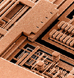
DE: So even with BSI, there are some structures on the back of the chip still?
DE: 所以就算是BSI,在芯片背面还是有一些结构?
JK: Some structures…
JK: 一些结构是……
The Samsung NX1 image sensor, shown under a magnifying lens.
DE: Because the well depth you’re talking about, the… are you talking…
DE: 因为你说到了井深。是指……你是在说……
JK: Distance to the photodiode from the…
JK: 从……到光电二极管的距离
DE: From the surface. But if it’s on the back, then I would think all the structures are on the front.
DE: 从表面。但如果光电二极管在背面,我觉得所有的结构都在正面(因为是背照式,所以DE认为背面应该没有结构,都放在正面,译者注)。
JK: You still have a CFA (color filter array), you still have some insulating layers, so there’s still some depth there.
JK: 你还有CFA(彩色滤镜阵列),还有一些绝缘层,所以这里还有一些深度。
DE: There’s still some depth there.
DE: 这里还有一些深度。(肯定JK的话,译者注)
JK: I’ll show you some illustrations out on the floor that’ll show you that the well depth’s about a third of what it is for front-side illuminated. Or not the well depth, but I’d say the light depth, so if you include the microlens in there, if you include the bonding layers, all that stuff, you’re looking at probably less than a third of the distance that you’d have on a similar structure, frontside-illuminated.
A comparison of frontside and backside-illuminated sensor structure.
DE: Yeah, and so there are other advantages to BSI as well, because it’s very shallow, in terms of the angle of incidence of light rays it can accept from the lens.
DE: 是的。所以BSI在接收镜头入射光的角度方面也一些优势,因为它很浅。
JK: Yes, it makes the microlenses much more efficient. You’re looking at about a 70% improvement in angle of light to the photodiode.
JK: 是的,它使微透镜变得更有效,你能观察到在一定入射角度下大约提升了70%。
DE: Wow, 70%. That’s really significant.
DE: 哇,70%,这很显著。
JK: Versus the sensor that’s in the NX30.
JK: 和NX30的传感器相比。
DE: Yeah. Now to some extent, the angle of the light, that’s a function of the lens, what it’s designed to put out in terms of the angle of the light rays that approach the sensor. But this might give you less shading, around the edges?
DE: 嗯。某种程度上来说,光线的角度是镜头在控制,在设计上会使光线的角度靠近传感器。这(BSI,译者注)可能给画面边缘带来更少的漂移?
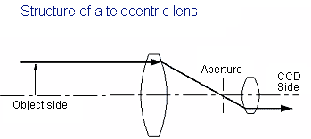
JK: Well, yes and no. That’s up to the lenses that you’re feeding the pixels with. It gives you an opportunity to use lenses that are less image-side telecentric… [Telecentricity refers to how close light rays coming from the lens are to perpendicular as they contact the sensor.]
JK: So in the last… long time, the last ten years-ish or so, as manufacturers have been building more digital lenses, they’ve been focusing on supporting microlenses with image-side telecentric light presentation…
Telecentric lenses are designed so light rays will enter the sensor straight-on. This helps avoid problems around the edges and corners of the sensor caused by shading due to the deep 3-D structure of the pixel circuitry, as well as aberrations resulting from the light striking the microlenses at an angle. Image courtesy Keyence Vision Systems.
JK: You don’t necessarily have to do that, you don’t have to do that as much with this lens. You’re not going to get the falloff, you’re not going to get some of the color fringing that you get from bleed between pixels, and CFA pollution. That being said, most of the lenses that are on the market now, especially the ones from us, have been designed to already present the light relatively straight to the surface of the image sensor, so if it’s already presenting the light straight that’s fantastic with these backside-illumination structures, and it makes them even more efficient at collecting light.
DE: And I guess if this BSI technology propagates across the NX line, then that would give your lens designers more latitude too, in that they don’t have to be constrained by the need for telecentricity?
DE: 我想如果这个BSI技术在整个NX产品线上得到使用,也会给你们的镜头设计师们更大的自由,因为不必受限于远心的要求?
JK: It could. I don’t know that we’d take that opportunity, though. All this work that’s gone on in the last few years across the industry in making the lenses better is still the right way to go, and I would assume and hope that that’s the way most of the industry continues to go.


Leave a Reply